Electronic Devices and Circuit Theory, section one
Nearly all the text here is copied from the book "Electronic Devices and Circuit Theory, 11th edition."
Semiconductor Devices
- The first integrated circuit was developed by Jack Kilby while working at Texas Instruments in 1958.
- Materials commonly used in the development of semiconductor devices: Silicon, Germanium, Gallium Arsenide.
- The farther an electron is from the nucleus, the higher is the energy state, and any electron that has left its parent atom has a higher energy state than any electron in the atomic structure.
Energy Levels
- In insulator, the energy gap (also known as forbidden band) between conduction band and valance band is bigger than 5 eV. That's the reason why its electrons cannot move freely. For conductors, the conduction band and valance band is overlapped. Also, it is the mechanism that make conductors' electrical properties. For semiconductor materials, energy gap is different according to the material itself.
- $E_g = 0.67 eV$ (Ge)
- $E_g = 1.1 eV$ (Si)
- $E_g = 1.43 eV$ (GaAs)
- An electron in the valence band of silicon must absorb more energy than one in the valence band of germanium to become a free carrier. Similarly, an electron in the valence band of gallium arsenide must gain more energy than one in silicon or germanium to enter the conduction band.
- What is electron Volts, see from the equations:
$$
V = \frac{W}{Q}\
W = QV\
= (1.6 \cdot 10^{-19}\ \text{C})(1\ \text{V}) \
= 1.6 \cdot 10^{-19}\ \text{J}
$$
$$
\text{So that,}\
1\ \text{eV} = 1.6 \cdot 10^{-19}\ \text{J}
$$
n-type and p-type Materials
- A semiconductor material that has been subjected to the doping process is called an
extrinsic material. - Both n-type and p-type materials are formed by adding a predetermined number of impurity atoms to a silicon base. An n -type material is created by introducing impurity elements that have five valence electrons (pentavalent), such as antimony, arsenic, and phosphorus.
- Note: It is important to realise that even though a large number of free carriers have been established in the n -type material, it is still electrically neutral since ideally the number of positively charged protons in the nuclei is still equal to the number of free and orbiting negatively charged electrons in the structure.
- The p-type material is formed by doping a pure germanium or silicon crystal with impurity atoms having three valence electrons. The elements most frequently used for this purpose are boron, gallium, and indium.
- Note that there is now an insufficient number of electrons to complete the covalent bonds of the newly formed lattice. The resulting vacancy is called a hole and is represented by a small circle or a plus sign, indicating the absence of a negative charge.
Electron versus Hole Flow
The effect of the hole on conduction is shown in Fig. 1.10 . If a valence electron acquires sufficient kinetic energy to break its covalent bond and fills the void created by a hole, then a vacancy, or hole, will be created in the covalent bond that released the electron. There is, therefore, a transfer of holes to the left and electrons to the right, as shown in Fig. 1.10. The direction to be used in this text is that of conventional flow , which is indicated by the direction of hole flow.
Note to reader who hasn't got the book: Figure 1.10 is something like bellow.

- In an n-type material the electron is called the majority carrier and the hole the minority carrier. In a p-type material the hole is the majority carrier and the electron is the minority carrier.
Semiconductor Diode
- This region of uncovered positive and negative ions is called the depletion region due to the “depletion” of free carriers in the region.
- The term bias refers to the application of an external voltage across the two terminals of the device to extract a response.

- Reverse-bias condition: If an external potential of V volts is applied across the p–n junction such that the positive terminal is connected to the n-type material and the negative terminal is connected to the p-type material, the number of uncovered positive ions in the depletion region of the n -type material will increase due to the large number of free electrons drawn to the positive potential of the applied voltage. This widening of the depletion region will establish too great a barrier for the majority carriers to overcome, effectively reducing the majority carrier flow to zero.
- The number of minority carriers, however, entering the depletion region will not change, resulting in minority-carrier flow vectors of the same magnitude with no applied voltage. The current that exists under reverse-bias conditions is called the reverse saturation current and is represented by $I_s$.
- Forward-Bias condition: A forward-bias or “on” condition is established by applying the positive potential to the p-type material and the negative potential to the n-type material. The application of a forward-bias potential $V_D$ will “pressure” electrons in the n-type material and holes in the p -type material to recombine with the ions near the boundary and reduce the width of the depletion region. As the applied bias increases in magnitude, the depletion region will continue to decrease in width until a flood of electrons can pass through the junction, resulting in an exponential rise in current.
Shockley's Equation - Diode Current Formula
$$
I_D = I_S (e^{V_D/nV_T}- 1)\ \text{[A]}\
\approx I_S \cdot e^{V_D/nV_T} \text{ ($V_D$ positive)}
$$
where
- $I_s$ is the reverse saturation current,
- $V_D$ is the applied forward-bias voltage across the diode,
- $n$ is an ideality factor, it has range between 1 and 2,
- $V_T$ is thermal voltage and can be determined by the equation follows:
$$
V_T = \frac{k\cdot T_K}{q}\ \text{[V]}
$$
where
- $k$ is Boltzmann's constant $= 1.38 \cdot 10^{-23}\ \text{J/K}$,
- $T_K$ is the absolute temperature in kelvins,
- $q$ is the magnitude of electronic charge.
- The reverse-bias potential that results in this dramatic change in characteristics is called the breakdown potential and is given the label $V_{BV}$.
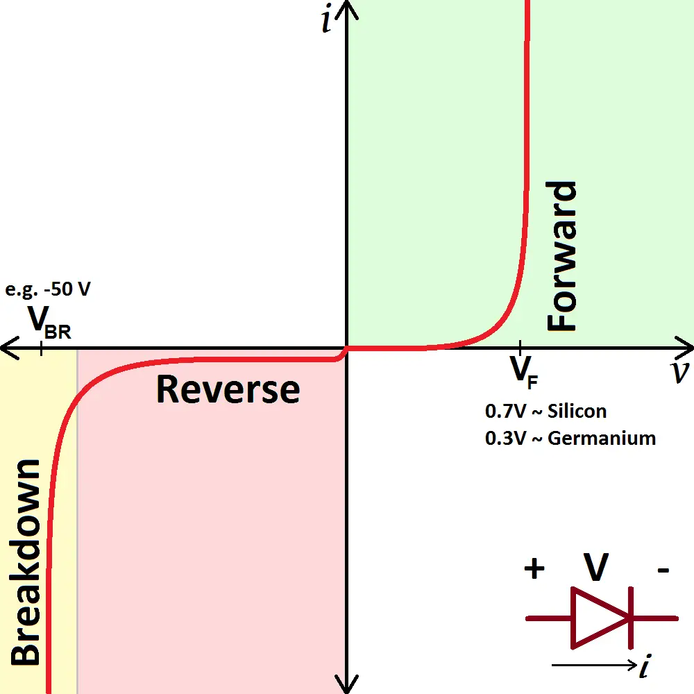
- The maximum reverse-bias potential that can be applied before entering the break-down region is called the peak inverse voltage (referred to simply as the PIV rating) or the peak reverse voltage (denoted the PRV rating).
- The reverse breakdown voltage of a semiconductor diode will increase or decrease with temperature.
- In general, therefore, the higher the current through a diode, the lower is the dc resistance level.
Diode Specification Sheets
- The forward voltage $V_F$,
- The maximum forward current $I_F$,
- The reverse saturation current $I_R$,
- The reverse-voltage rating PIV, PRV or V(BR),
- The maximum power dissipation level at a particular temperature, $P_{dissipated} \approx (0.7 \text{V})I_D$
- Capacitance levels,
- Reverse recovery time $t_{rr}$,
- Operating temperature range